OMCL-AC240TM Discontinued
OMCL-AC240TM-R3 / 100 chips, Reflex side aluminum coating
OMCL-AC240TM-B3 / 18 chips, Reflex side aluminum coating
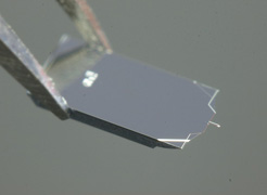
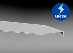
The new OMCL-AC240TM type 3 series with ‘New Concept Chip’
Platinum-deposited cantilever is suitable for electrical characterization application such as electric force microscopy (EFM), Kelvin probe force microscopy (KFM).
Outstanding features
- 1. Platinum coating for electrical measurement
- 2. The higher conductivity even with a sharper probe
(Common features in new silicon cantilever series)
- 3. Ideally point terminated probe
- 4. Acclaimed ‘TipView’ structure
- 5. Reflex side aluminum coating
- 6. Ease in chip handling: ‘New concept chip’
- 7. Packaging: Pre-separated chips
More about New OMCL-AC240TM type 3 series
1. Platinum coating for electrical measurement
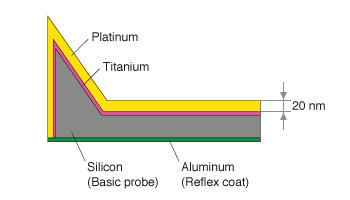
The platinum layer is deposited on the basic silicon probe with the titanium interfacial layer. The surfaces of precious metal coatings are free from oxidization and are electrically stable. The platinum layer on the probe has smooth surface, and the tip shape follows the shape of the basic silicon probe. Unprecedented probe sharpness of 15 nm (Nom.) in radius as a metal coated probe is worth trying in studying devices.
For more details, please refer to FAQs for platinum-deposited cantilevers.
2. The higher conductivity even with a sharper probe
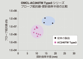
As can be seen in the graph below, OMCL-AC240TM type3 with tip side platinum coating shows higher conductivity while its probe is sharpened more than our conventional product. This probe reveals sample surface precisely both in electrically and in topographically.
3. Ideally point terminated probe
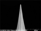
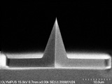
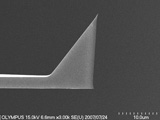
The apex of the tetrahedral probe is ideally point terminated. The tetrahedral probe shows good symmetry viewed from the front of the cantilever. Considering the geometric feature, choose the fast scan (X) direction. Check Scan line profile and enlarged view of the tip apex.
4. Acclaimed ‘TipView’ structure
The probe can be easily positioned at the exact point of your interest due to ‘TipView’ structure.
The probe is located at the exact end of the cantilever so that the probe apex is not obscured during optical observations.
5. Reflex side aluminum coating
Thin aluminum film with the thickness of 100 nm is deposited on the cantilever for reflecting light from the deflection sensor in the AFM equipment. High reflex for high S/N sensing can be expected.
6. Ease in chip handling: ‘New concept chip’
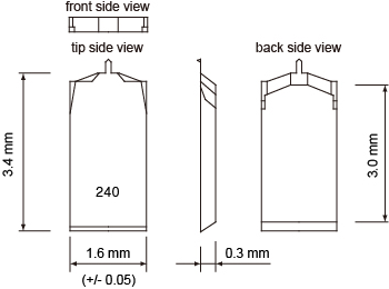
The ideally vertical side-walls of the chip make tweezing easy and eliminate problems with chipping and debris.
7. Packaging: Pre-separated chips
Silicon Cantilevers, model OMCL-ACxxxxx-R3: available with 100 pre-separated chips.
Silicon Cantilevers, model OMCL-ACxxxxx-B3: available with 18 pre-separated chips.
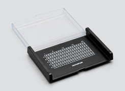
OMCL-AC240TM-R3
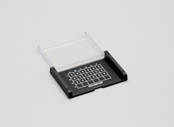
OMCL-AC240TM-B3
