Q&A
General information on Micro cantilevers
Q1. What is Atomic Force Microscope (AFM)?
Please click here to see basic idea of AFM.
Q2. What items do I need to remove a tip from a wafer?
Tweezers, a Thin stick, Both-side adhesive tape, a Razor blade (knife), Post-it tape and a Chip storage case.
Those could be found in your lab or office.
Dry box for chip storage
Please pay attention to the environment of where you store the chip. Ensure your tips are stored in a proper environment including correct storage box. The rest of your cantilever tips must be the heart component also for the next measurement.
Optical microscope for inspection
That would be of help to you to gain a better understanding of how cantilever and chips are connected. Cantilevers should be inspected under the microscope before use, especially if you are not familiar with OLYMPUS microcantilevers.
Anti-electrostatic discharge items
The sharper tip needs the more careful handling to prevent static damage to the tip. Use of an anti-electrostatic mat and a wristband are recommended likewise when handling laser diode chips. Handling under an ionizer is also recommended.
Please avoid wearing clothes like woolen sweaters, fleece etc when handling the cantilever cases and chips.
FAQs
Micro cantilevers for force curve measurements of soft samples( Bio-Lever )
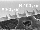
Q1. When approaching a wet sample (with the cantilevers still dry), the cantilevers may be sucked into the water by the surface tension at the interface. Sometimes, the cantilever, especially B-lever of "Bio-Lever" (100 um long, 0.006 N/m), can be bent down 90 degrees to the substrate making it impossible to get any reflected laser light.
Before approaching the cantilever toward the sample surface, wet both the sample and the cantilever.
Using a syringe, gently apply a drop of water to the cantilever holder from the side of the cantilever chip. This way the air-water interface approaches the cantilever sideways and the cantilever is less likely to bend.
FAQs
Micro cantilevers for electric measurement ( Platinum-deposited silicon cantilever with a tetrahedral tip )
Q1. With what voltage the break-down occur?
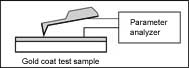
In our experiment using a gold-coated sample illustrated below, break-down occurred at 3 volts and 7 mA. In case of dielectric material, break-down wasn't found even at 50 volts. Note that the tip loading force was roughly regulated in those experiments.
Please understand that the break-down voltage is not guaranteed because measurements and samples are diversified.
Q2. How thick is the platinum coating around the probe apex?
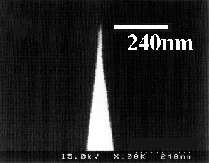
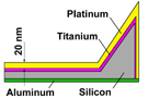
According to our recent experiment, the thickness of the platinum layer on the probe apex was estimated to be approximately 8 nm while the layer on flat surfaces was 20 nm thick.
The tip radius after platinum/titanium coating was 13.08 nm (ave.), which is sufficiently sharp, although a modest increase from that of the basic silicon probe, {4.68 nm (ave.)} is perceived.
Q3. Am I better to use platinum-deposited probe also in UHV-SPM?
In most of the cases, it is not necessary, I believe. Highly doped silicon probe is the best for UHV-SPM with a tip cleaning mechanism, at present.
Highly doped silicon probes are frequently used for electric measurements because of the relatively high conductivity and their sharp tip radius, which can be less than 10 nm. The native oxide layer formed on the surface of the probe when exposed to air sometimes complicated the data interpretation. But now researchers know that removing the oxide layer in the UHV chamber before scanning results in simple scheme of the tip and the sample in physics.
In case of measurements in which short time-constant of the circuit for probing electrical properties of samples is required, our sharp platinum-deposited probes would be better due to their high conductivity.
Q4. How large light-reflectance can be expected with aluminum reflex coating?
About 90%. It is twice as high as that for platinum reflex-coating and three times as high as that for raw silicon cantilever.
Q5. Is the OLYMPUS Electri-Lever available for electro-chemical measurements? I want to do experiments in strong acid or alkaline solutions.
Its use in the strong solutions is not recommended because aluminum for reflex coating dissolves.
FAQs
Micro cantilevers for AC (dynamic) mode AFM
( Silicon cantilever with a tetrahedral silicon tip )
Q1. Why is silicon chosen for the tip material for the cantilevers for AC mode AFM?
Because silicon is suitable to form the sharpest tip.
Q2. Isn't a silicon tip easy to break?
Yes. Considering the tip sharpness and material, a silicon tip might break easier than a silicon nitride tip. However, tip loading force in AC mode AFM is smaller than in DC mode AFM, so the silicon tip works well in AC mode AFM.
Please be careful.
Q3. How do we know when a tip is broken?
A tip broken and tip wear should be known as a different phenomenon.
Tip wear gradually progresses during the measurement. The tip shape will change to dull (blunt). This may be hard to determine however the large change may be suspected when degradation image appears after scanning.
A broken tip often occurs after accidental clash in the tip engagement (approaching) procedure before the scanning. A twin probe image will appear in the AFM image when the tip is broken. Every cross sectional shape of the tetrahedral tip is triangle. So an overlapped image of two or three shifted image will be observed. Operators should care about the speed of the tip engagement.
The change of the tip shape may be due to either/or a broken and a tip wear. Operators should optimize the condition of their feedback control and examine the tip shape periodically using a standard specimen.
Q4. Does the tetrahedral shape of the tip give any influence to AFM images?
No matter what shape of a tip has a possibility of giving marks to AFM images. Some triangle marks might appear in the image with the tetrahedral tip.
Q5. What is the deviation of mechanical properties of the OMCL-AC series cantilever?
Stiffness and resonant frequency of each cantilever in the data sheet are calculated values. Please allow the deviation of plus/minus 20 % on the resonant frequency, plus75% and minus 50% on the stiffness.
Q6. What is the light reflectance of the silicon cantilever without the reflect coating?
It is about 25% for the visible light. Even with such small reflectance, non coated cantilever (OMCL-AC160BN-) will work in most of the AFM instruments available in the market.
So, choose OMCL-AC160BN- if you care the backside coating material (Aluminum).
Q7. Does the infrared light pass through the silicon cantilever tip?
Yes.
Silicon (non-dope) with the thickness of about 1mm shows transparency of about 50% for the IR light of 1.2 um -- 8 um. IR light in that range can go through the silicon cantilever and/or tip (OMCL-AC160BN-: non-coat cantilever) because the cantilever and tip are thin.
Q8. Does OLYMPUS have highly doped silicon cantilevers? I am interested in STM/AFM simultaneous measurement.
It's not available, however OLYMPUS offers a platinum-deposited probe; OMCL-AC240TM- as its alternative.
Silicon tip cantilevers in OMCL-AC series are made of n-type single crystal silicon lightly doped with phosphorus that is a semiconductor material and the tip surface is covered with natural oxide layer. So OLYMPUS asks metal coating in customer side for the use.
illustration of Pt deposited probe Most of doped silicon cantilever probes from others have also covered with natural oxide layer. So if you can allow the tip radius increase, platinum-deposited probe; OMCL-AC240TM- is recommended.
Q9. In tuning the cantilever-drive-frequency before scanning, a sub-peak was appeared beside the main peak at first resonant frequency in the vibration spectrum. The shape of the main peak was not sharp comparing to the shape without sub-peak. Is there any idea to make it better?
Clean the chip holder with an absorbent cotton to improve mechanical vibration coupling between the chip substrate and the chip holder with an actuation piezo. Avoid sandwiching pieces of small shards with the cantilever chip and the chip holder.
Be sure to press the center of the chip substrate in the chip holder. In pressing one third of the chip, the vibration spectrum sometimes gets out of the shape.
FAQs
Micro cantilevers with high aspect ratio tip for AC (dynamic) mode AFM
( Silicon cantilever with a blade-like tetrahedral tip )
Q1. Will the Blade tetra tip give the high aspect ratio in all directions?
No. But, most of the normal high aspect tips make them all asymmetric for high aspect ratio applications because of the chip mounting angle. In viewing from the front, the Blade tetra tip is symmetric with the tip angle of about 12 degrees. In viewing from the side, the tip is inclined or asymmetric. The tip angle is macroscopically 35 degrees or less and microscopically about 25 degrees. So, this type of the tip will not give the high aspect ratio in all directions. Actually, estimating the tip diameter (shape) by a tip-shape-qualification software, elliptical cross section of the tip appears by the distance from the tip apex. Therefore, good results can be expected when aligning our cantilever along the grooves in the gratings, DVD pits. (see image)
FAQs
Micro cantilevers for AC (dynamic) mode AFM
( Silicon nitride cantilever with a wedge shaped silicon nitride tip )
Q1. Why is silicon nitride chosen for the tip material for the cantilevers for AC mode AFM?
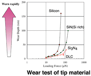
First because silicon nitride tip is hard to wear compared with silicon tip which is the most popular tip for AC mode measurement (see left graph). OMCL-HA100WS- series employs Si3N4, or stoichiometric silicon nitride as the tip material. And secondly, silicon nitride is one of the most popular materials in the silicon process. So good cost performance can be achieved.
Q2. What is the SiN sharpened wedge tip mainly used for?
This tip is recommended as a probe for the inspection procedure of the products that have surface roughness smaller than 200 nm. For measuring polycrystalline silicon film that is used in semiconductor IC, hard and sharp tip is required for stable measurement.
Needs for the low wear tip must increase because many customers would like to use AFM as a tool for the inspection of the products and expect reliable inspection system.
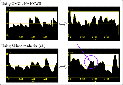
Q3. I understand that Si3N4 film is hard material in the graph above, but is there any data of long tip lifetime?
Variation of the line scan profiles with Si3N4 tip and Silicon tip are shown below. The line profiles are the first and tenth images after repeating the measurement (repeating engage procedures) of rugged titanium film and silicon made mesh-pattern sample. Although a series of acceleration tests had been done, each condition on the servo feedback is optimized as well as normal AFM measurement when the line profile data (images below) were taken.
After the tenth image of the silicon made tip is obtained, you can see rounded line profile because of tip wearing (blue circle). The sharp protrusions as in the first image disappeared because of tip wear.
FAQs
Micro cantilevers for DC (contact) mode AFM
Q1. Why is silicon nitride chosen for the tip material for the cantilevers for the contact mode AFM?
Simply saying, because silicon nitride is a generally used material in silicon IC process.
Q2. Is there any advantage in a silicon nitride tip?
Yes. The silicon nitride tip is recommended for stable AFM measurement in contact mode, since silicon nitride tip is hard to wear compared with silicon tip (see right). Large tip force is loaded to a sample surface in contact mode AFM in air because of the contamination layers on the tip and the sample. This may cause tip wear, so harder material tip is preferable.
Q3. Does the silicon nitride tip give a good result for all samples?
The silicon nitride tip works for most of samples. There are still some exceptions. If you measure a silicon nitride sample in contact mode AFM with the silicon nitride tip, sometimes AFM images are distorted.
Q4. Is there any treatment for changing a silicon nitride tip into hydrophilic?
Try to expose the tip with UV light.
Or, if you have a oxygen plasma reactor, try it. That is the way to change the tip surface in a short time. In our experience, 10 sec is enough to change it.
Q5. Is there any treatment for changing a silicon nitride tip into hydrophobic?
Coating a tip with silane coupler was reported in a conference.
Q6. I am interested in silane treatment for silicon nitride probe. How much oxygen is contained on the surface?
According to the result of our latest XPS analysis of silicon nitride film for OLYMPUS cantilever, Silicon, Nitrogen, Oxygen and Carbon are detected on the surface of the film. Our silicon nitride is silicon-riched for reducing the internal film stress.
Carbon is due to the contamination layer on the silicon nitride film and its concentration is 11.6%. The carbon is reduced less than 5% by oxygen plasma treatment. Similar reduction is observed by H2SO4 + H2O2. Ethanol works a little to remove carbon from the contamination. 8% of carbon is detected after the ethanol rinsing.
Our silicon-rich silicon nitride film contains oxygen and the concentration is less than that of glass, or silicon dioxide. The concentration of oxygen is 10 percents or more and it is one fourth to one fifth of that in glass. This means silane treatment can be done fundamentally.
Q7. What kind of attention should customers pay to add a coating on the cantilever?
Stress control of the coating is it! Soft cantilevers would easily bend by coating. If you have not any experience with the coating, you should choose stiffer cantilevers to start with.
Of course, you should take good care to the tip sharpness.
Good luck in your lab.!
Q8. Which type of the cantilever is suitable for AC mode AFM in water?
For AC mode AFM operation in water, the short cantilever (100um long) in OMCL-TR400PSA- is recommended.
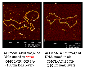
The customer who has successfully taken a DNA image in air with OMCL-AC120TS- (right image in left), must have confidence in oneself on the sample treatment.
Then try it in water with OMCL-TR400PSA- !
Both images (left) are taken by OLYMPUS NVB100 (SPM for biology).
OMCL-TR400PSA- has two types of cantilevers, 100 um long and 200 um long. The resonant frequencies of those cantilevers shift lower to about 7 kHz and 3 kHz in water respectively however they are 34 kHz and 11 kHz in air. Because 3 kHz is low, it must be close to the resonant frequency of the scanner in your SPM instrument.